Components & Pinouts
warning
This section is still under heavy construction, content will often be added and changed.
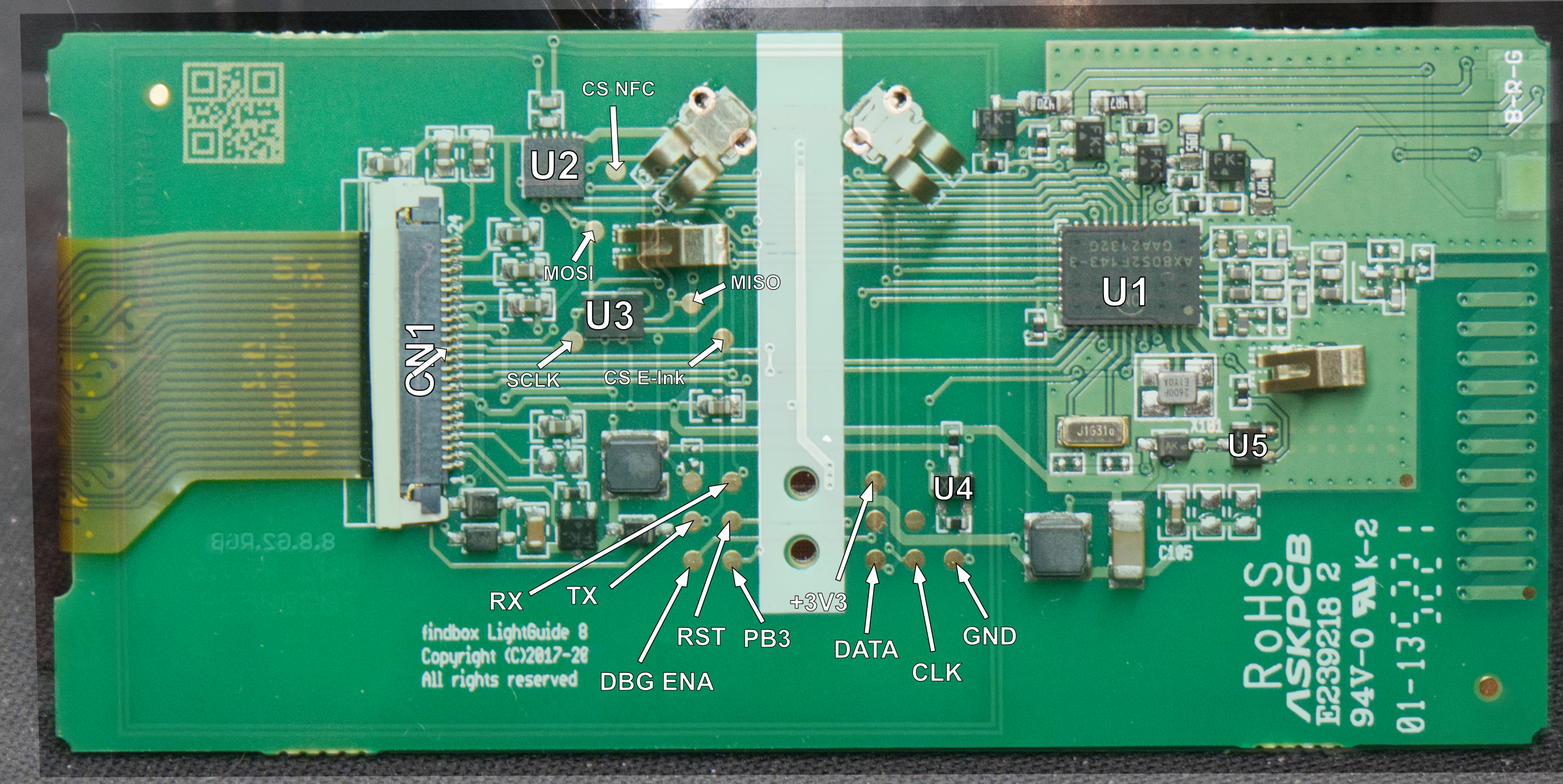
Main Components
| ID | Part | Function | Description | Link |
|---|---|---|---|---|
| U1 | AX8052F143 | MCU | 8-bit 8051 MCU with integrated radio | Datasheet |
| U2 | FM11NT081DS | NFC | NFC Forum Type 2 Tag IC | Datasheet |
| U3 | T.B.D | Flash | 1Mb Serial Flash Memory | - |
| CN1 | GDEW026Z39 | Display | 2.6" E-ink display module | Datasheet |
AX8052 Wireless MCU (U1)
I'll create a markdown table with all the pin connections organized according to your requested headers.
| MCU Pin | Device/Bus | Signal name | Description |
|---|---|---|---|
| PA0 | E-Ink | D/C | Data/Command signal |
| PA1 | SPI | CS | E-Ink chip select |
| PA2 | - | Connected to Transistor U5 | |
| PA3 | P | Crystal Oscillator positive terminal | |
| PA4 | N | Crystal Oscillator negative terminal | |
| PA5 | - | Connected to Transistor U4 | |
| PB0 | LED | - | White LED control |
| PB1 | SPI | CS | NFC chip select |
| PB2 | E-Ink | BUSY | E-Ink busy status signal |
| PB3 | BOOT/NFC | FD | Bootloader and NFC Field Detection |
| PB4 | UART | TX | UART transmit |
| PB5 | UART/E-Ink | RX/RST | UART receive and E-Ink reset |
| PB6 | LED | - | Green LED channel |
| PB7 | LED | - | Blue LED channel |
| PC0 | SPI | CS | FLASH chip select |
| PC1 | SPI | SCLK | SPI clock |
| PC2 | SPI | MOSI | SPI master out slave in |
| PC3 | SPI | MISO | SPI master in slave out |
| PC4 | LED | - | Red LED channel |