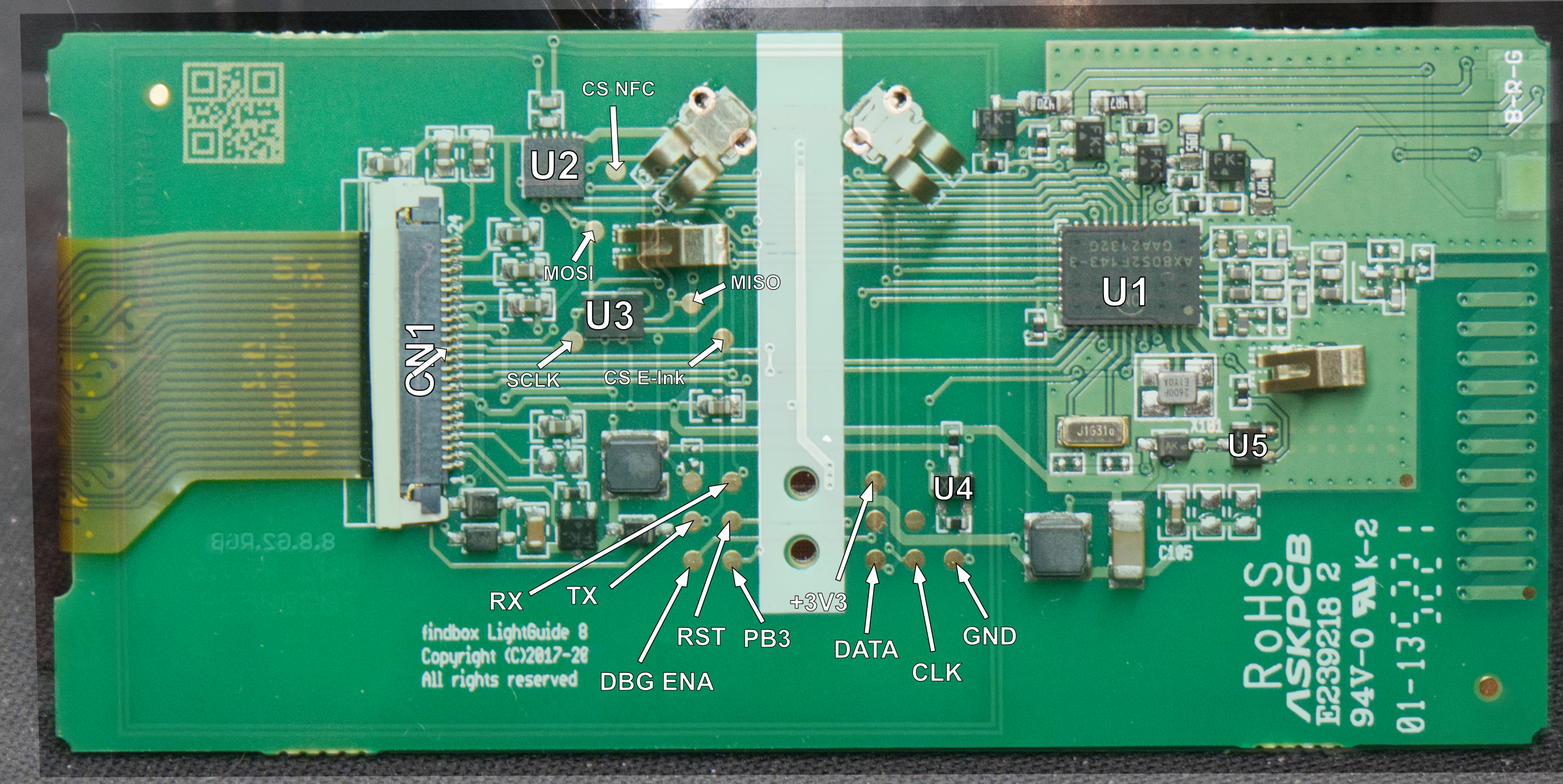
PCB Overview
The PCB is a fairly generic board like every other electronic shelf tag
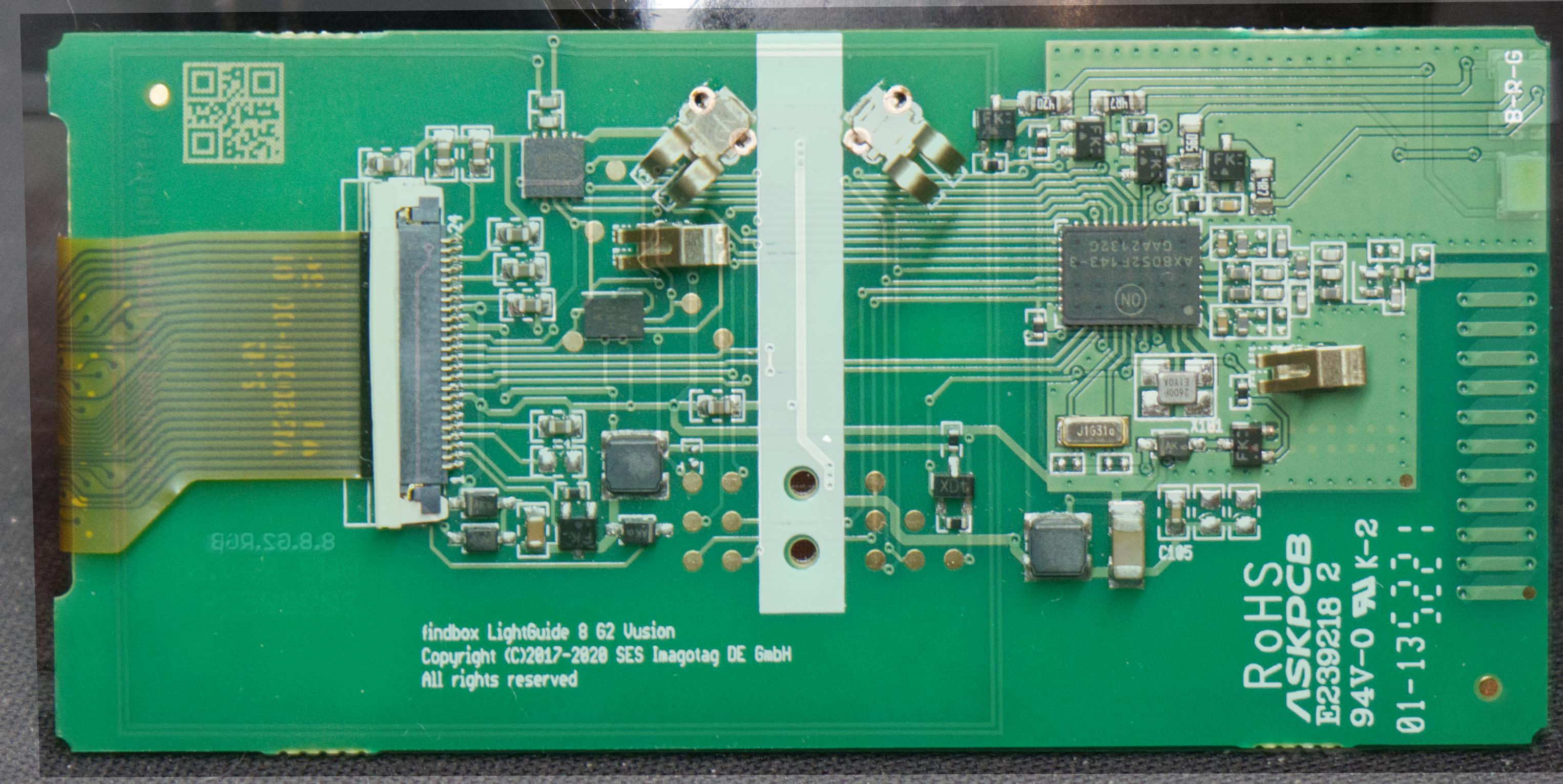
Taking photo's of both the front and back of the PCB allowed me to create the following X-Ray-like image of the PCB by overlaying them in a photo editor and making the front layer a bit transparent. This way I could see where the traces on the front layer went and where they connected to on the back layer. Since this is just a 2 layer board, this was fairly easy to do.
further analysis and processing resulted in the following board overview. The signals were determined mostly by checking the datasheets of the different components and tracing the signals from the MCU to the different components. After that just logically determine what each pin does and what signal it is. Some signals were still left over, however as soon as i had the toolchain up and running with custom bootloader, just uploading a simple blinky program and checking the signals with a scope was enough to determine what the signals were.